

2026-11-12
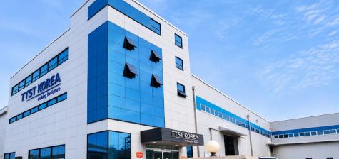
从产品出海到制造出海|TTST Korea 制造基地研究所 正式开业启航!
阅读全文


强化韩国本土研发,打造“中韩合作标杆”
韩国是全球高端PCB、半导体与AI载板的核心产业高地。韩国工厂的落成是公司“制造走向国际”的历史性一步。面向AI算力厚板、IC载板(FC-BGA)、玻璃基载板及半导体等设备的发展需求,公司需贴近全球顶尖技术生态,因此在韩国本土建立研发中心,吸纳当地工程人才,围绕下一代先进封装和载板设备开展深度研发,推动韩国制研基地成为TTST全球技术创新的重要引擎。
Korea is a key global hub for high-end PCB, semiconductor, and AI substrate industries. The Korea factory represents a major step in TTST's global manufacturing strategy. To meet equipment requirements for AI computing thick boards,FC-BGA IC substrates,glass core substrates,and semiconductors, we need to stay close to leading technology communities. That is why we established this local R&D center in Korea and hired local engineers to develop next-generation equipments for advanced packaging and substrates. This Korean site will become an important global innovation hub for TTST.
深耕高端PCB与载板装备,推进全球化产业协同
TTST Korea制造基地研究所,将提供TTST全产品线的本地销售与服务,把韩国制造基地研究所的工匠精神与研发底蕴,与中国高效制造及自动化技术相结合,共同推动全球泛半导体产业进步。
TTST Korea Manufacturing Base & Research Institute provides local sales and service for all TTST products. It combines Korea's R&D strengths with China's efficient manufacturing and automation technology to support the development of the global pan-semiconductor industry.
● TTST自 2018 年成立以来,长期深耕HDI-mSAP、AI算力板、IC载板、玻璃基载板、先进封装、半导体领域。目前公司聚焦两大核心方向:在AI算力厚板领域:裁磨线、冲孔机、塞孔机、高纵横比电镀线、高精度压机等设备市占率领先; 在细线路领域:VCP电镀线、Coreless分板机、垂直显影/蚀刻/去膜、高精度压机、ABF撕膜机、撕铜箔机、烤箱等满足前沿工艺需求。
Founded in 2018, TTST focuses on HDI-mSAP, AI computing boards, IC substrates, glass core substrates, advanced packaging, and semiconductors. The company focuses on two core technology areas:AI Computing High-Layer-Count PCBs: TTST holds a leading market position in equipment for Trimming & Grinding lines, Post-etch punching machines, and Vacuum resin plugging machines, High aspect ratio board electroplating, as well as High-precision press machine. Fine-Line Processing: TTST provides VCP plating ,Coreless detach machine and Vertical developing
/etching/stripping (DES) systems、High-precision press machine, ABF peeling machine, Carrier copper foil peeling machine, Oven to meet the requirements of advanced fine-line processes.Keep innovating, improve our equipment and integrated process solutions, and steadily expand our global layout.
在AI算力、先进封装与高端载板产业加速演进的背景下,设备企业全球化正从单一产品输出转向制造、服务与研发验证的本地化协同。TTST韩国制造基地研究所的开业,意味着其正以中韩产业技术协同为支点,进一步强化面向高端PCB及半导体载板客户的全球化服务响应能力。与海内外客户伙伴抢抓AI与半导体产业发展机遇,共创产业新价值!
As AI computing, advanced packaging, and high-end substrate industries grow rapidly, equipment suppliers are moving beyond simple product sales toward local manufacturing, service, and R&D support. The opening of the TTST Korea site enables us to leverage China-Korea technical synergy and respond faster to high-end PCB and semiconductor substrate customers worldwide. We will work with all partners to capture opportunities in the AI and semiconductor sectors and create greater value together.


